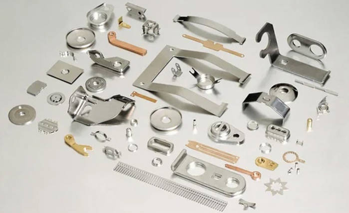
RF shields may look like simple stamped metal covers, but small differences in flatness, material thickness, frame fit and soldering surfaces can create serious problems during PCB assembly.
For purchasing teams and engineers, the real challenge is not finding a supplier who can stamp the part. It is finding one who can maintain dimensional consistency from prototype to mass production.
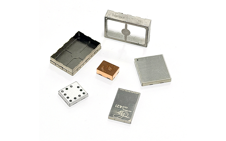
1.What are the primary application areas for rf shielding cans?
- Consumer Electronics: smartphones, tablets, smart watches, TWS earbuds, routers & set‑top boxes
- Telecommunication: 4G/5G communication modules, CPE, base station internal boards
- IoT & Smart Home: BLE / LoRa / NB‑IoT wireless sensors, smart gateways
- Automotive Electronics: T‑BOX, in‑vehicle WiFi / Bluetooth, radar modules
- Industrial & Medical Electronics: industrial wireless modules, portable medical instruments
- Security Products: GPS/Beidou positioning modules, walkie‑talkies
Functions of Shielding Cans
- Electromagnetic shielding
- Mechanical Protection
- Auxiliary Heat Dissipation
- EMC Compliance
2.What are the typical structures of RF shield ?
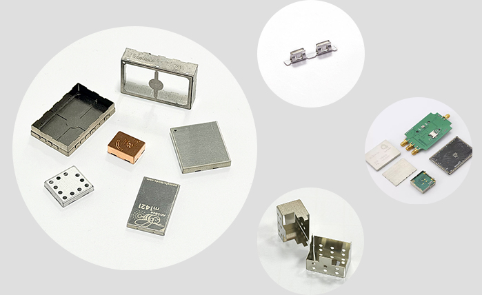
One‑piece rf shield can
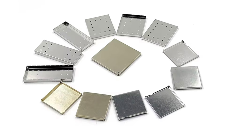
A one-piece RF shielding can is a metal shielding structure soldered directly onto a PCB. Its solder tabs or bottom edges are attached to the PCB’s ground pads without requiring a separate frame. It is suitable for electronic components that require protection against electromagnetic interference but do not need to be opened for maintenance after assembly.
Two‑piece rf shield can
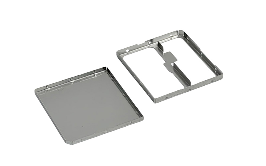
A two-piece RF shielding can, also known as a two-piece EMI shield or shielding frame and cover, consists of a metal frame soldered to the PCB and a removable cover. Unlike a one-piece shielding can, this design allows engineers to remove the cover to inspect, test, or repair the enclosed electronic components without desoldering the frame from the PCB.
The frame and cover are typically secured using one of the following four methods:
- Dimple Snap-Fit
Small dimples are stamped into the sidewalls of the frame or cover, while corresponding holes are formed in the mating part. Elastic deformation creates a secure locking force between the frame and cover. This is the most common fastening method.
- Undercut Structure
Local bending or undercut features prevent the top cover from accidental detachment. This fixing method is suitable for scenarios with severe vibration.
- Friction Fit
Clamping force is generated by controlling the dimensional tolerance between the frame and top cover. The structure is simple, yet it requires high stamping precision.
- Spring-Clip Fastening
Flexible contact tabs are designed into the sidewalls of the frame, allowing the cover to be repeatedly removed and reinstalled while maintaining reliable electrical contact. This design facilitates testing, adjustment, and maintenance.
Multi-Cavity Structure
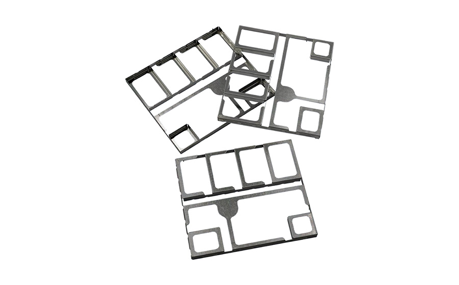
The multi‑cavity shielding can partitions a single shield into several independent compartments, enabling isolation for RF, power and sensitive electronic circuits within the same PCB area. Internal partitions help reduce electromagnetic coupling and crosstalk between adjacent components while saving PCB space.
3.How to Choose the Right RF shield Material for Your PCB?
Choosing an RF shield material requires more than a simple price comparison.
The metal affects shielding performance, solderability, corrosion resistance, mechanical strength, forming accuracy, and production cost. In addition, it influences SMT assembly and long-term product reliability.
Manufacturers commonly use nickel silver, tin-plated steel, stainless steel, copper, phosphor bronze, and brass. However, each option offers different advantages. Therefore, engineers must match the material to the PCB layout, operating environment, assembly process, and order quantity.
Quick Comparison of RF Shield Materials
| Material | Shielding | Solderability | Corrosion Resistance | Formability | Cost Efficiency | Best For |
|---|---|---|---|---|---|---|
| Nickel Silver | ★★★★☆ | ★★★★★ | ★★★★★ | ★★★★★ | ★★★☆☆ | Precision PCB shields and wireless modules |
| Tin-Plated Steel (SPTE) | ★★★★☆ | ★★★★★ | ★★★☆☆ | ★★★★☆ | ★★★★★ | Cost-effective mass production |
| Stainless Steel | ★★★☆☆ | ★★☆☆☆ | ★★★★★ | ★★★☆☆ | ★★★☆☆ | Automotive and harsh environments |
| Copper | ★★★★★ | ★★★★★ | ★★★☆☆ | ★★★★★ | ★★☆☆☆ | High-frequency and sensitive RF circuits |
| Phosphor Bronze | ★★★★☆ | ★★★★☆ | ★★★★☆ | ★★★★★ | ★★★☆☆ | Removable covers and spring contacts |
| Brass | ★★★★☆ | ★★★★☆ | ★★★★☆ | ★★★★☆ | ★★★☆☆ | Electrical hardware and special shield designs |
4.Which RF Shield Materials Need Electroplating?
Manufacturers use electroplating to deposit a thin metallic coating on the surface of an RF shield. This coating can improve solderability, corrosion resistance, electrical contact, wear resistance, and appearance.
However, not every shielding material requires additional plating. Therefore, engineers should select the surface finish according to the base material and application.
RF Shield Material and Plating Guide
1. Nickel Silver
Nickel silver usually does not require additional plating. It already offers good corrosion resistance, a stable surface, and excellent solderability.
Therefore, manufacturers often use bare nickel silver for precision RF shields. In addition, avoiding plating can shorten lead times and reduce the risk of coating-related dimensional changes.
However, some projects may still require tin, nickel, silver, or gold plating for special contact, appearance, or environmental requirements.
The Copper Development Association rates C75200 nickel silver as having excellent solderability and cold-forming capability. CDA C75200 material data
2. Tin-Plated Steel—SPTE
SPTE already consists of a steel substrate with an electrolytic tin coating. Therefore, it normally does not need another plating process before SMT assembly.
The tin surface provides good solderability and corrosion protection. Moreover, SPTE offers high strength and competitive material costs.
However, stamping exposes the steel substrate along cut edges. Consequently, harsh or humid environments may require additional tin plating or another protective treatment after stamping.
JFE Steel confirms that tinplate offers excellent solderability, formability, strength, and corrosion resistance. JFE Steel tinplate data
3. Stainless Steel
Stainless steel provides excellent strength and corrosion resistance. However, its passive oxide layer reduces solder wettability.
Therefore, an SMT shield frame made from stainless steel usually needs a solderable finish. Manufacturers often apply a nickel underlayer followed by tin plating.
In contrast, a removable stainless steel cover may not require plating if it does not connect directly to the PCB solder pads. Nevertheless, the contact points must maintain reliable electrical continuity with the frame.
4. Copper
Copper offers excellent electrical and thermal conductivity. However, its surface oxidizes when it contacts air and moisture.
Therefore, manufacturers commonly apply tin or nickel plating to copper shielding cans. Tin supports SMT soldering, while nickel improves wear and corrosion resistance.
Silver or gold can support specialized electrical applications. Nevertheless, these finishes increase the total cost.
The Copper Development Association lists C11000 copper with excellent solderability and cold-forming performance. CDA C11000 material data
5. Phosphor Bronze
Phosphor bronze provides good conductivity, elasticity, and fatigue resistance. Consequently, manufacturers often use it for removable covers, spring tabs, and grounding contacts.
Bare phosphor bronze can work in controlled environments. However, tin plating improves solderability, while nickel or gold supports repeated electrical contact and long-term stability.
The Copper Development Association rates C51000 phosphor bronze as having excellent solderability and cold-forming capability. CDA C51000 material data
6. Brass
Brass offers good formability, moderate conductivity, and excellent solderability. However, its surface may oxidize or discolor over time.
Therefore, manufacturers often apply tin plating when the shield requires PCB soldering. Alternatively, nickel plating can improve corrosion and wear resistance.
The Copper Development Association rates C26000 brass as having excellent solderability and cold-working capability. CDA C26000 material data
Common Plating Options
- Tin plating: Improves solderability and offers a competitive cost.
- Nickel plating: Improves corrosion resistance, hardness, and wear resistance.
- Silver plating: Provides high electrical conductivity for specialized RF applications.
- Gold plating: Maintains stable contact resistance and strong corrosion resistance, but increases cost.
Important Design Considerations
Plating adds thickness to the shield surface. Therefore, engineers should define the coating thickness before confirming the final drawing.
In addition, excessive or uneven coating may affect:
- Dimensional tolerances
- Frame-and-cover fit
- Snap-fit retention force
- Spring-contact performance
- Coplanarity
- SMT soldering consistency
For this reason, KAIYAN reviews the base material, finish type, coating thickness, tolerance, and application before production. This approach helps customers achieve reliable soldering and corrosion protection without adding unnecessary processing costs.
5.Customer Pain Points and Manufacturing Challenges of RF shields
In RF shield manufacturing, controlling coplanarity presents one of the greatest challenges. Generally, standard shielding cans require coplanarity below 0.10 mm, while precision shielding cans often demand a tighter tolerance below 0.05 mm.
When the bottom-edge coplanarity exceeds 0.10 mm, some areas may fail to contact the solder paste properly. Consequently, the shield may develop incomplete or open solder joints, poor grounding continuity, increased RF leakage, and lower mechanical stability. In addition, uneven soldering can cause shield movement during reflow and increase inspection and rework costs.
What Factors Affect the Flatness of an RF Shield?
Five Key Factors That Affect RF Shield Flatness
- Material Thickness and Hardness
Thin or hard materials deform more easily and create greater springback during forming. - Structural Design
Large surfaces, asymmetrical openings, and insufficient reinforcing ribs can reduce structural stability. - Forming Sequence and Springback
An incorrect bending sequence can redistribute internal stress and cause uneven bottom edges. - Tooling Accuracy and Wear
Uneven die clearance, poor alignment, and worn tooling can create dimensional variation and warping. - Packaging and Transportation
Stacking pressure, part nesting, and improper packaging can deform qualified shields after production.
How Does KAIYAN Control RF Shield Coplanarity?
KAIYAN Hardware controls coplanarity throughout the entire manufacturing process. For suitable shield dimensions and structures, we can achieve a coplanarity tolerance of ≤0.05 mm.
1.DFM Review Before Production
First, our engineers review the shield dimensions, wall height, openings, bend positions, and PCB soldering areas. As a result, we can identify deformation risks before tooling development.
2.Precision Stamping die Development
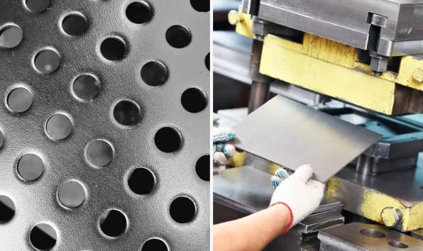
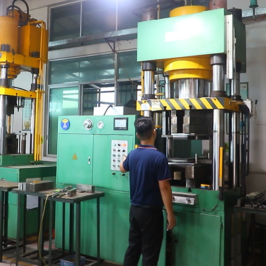
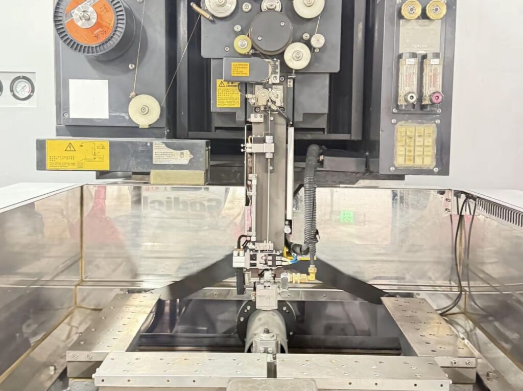
Once we confirm the final product drawing, our tooling team selects the progressive stamping die material and wire EDM method according to the order volume and precision requirements. Therefore, we can maintain consistent quality and dimensional accuracy while helping customers reduce tooling costs.
3.100% Inspection
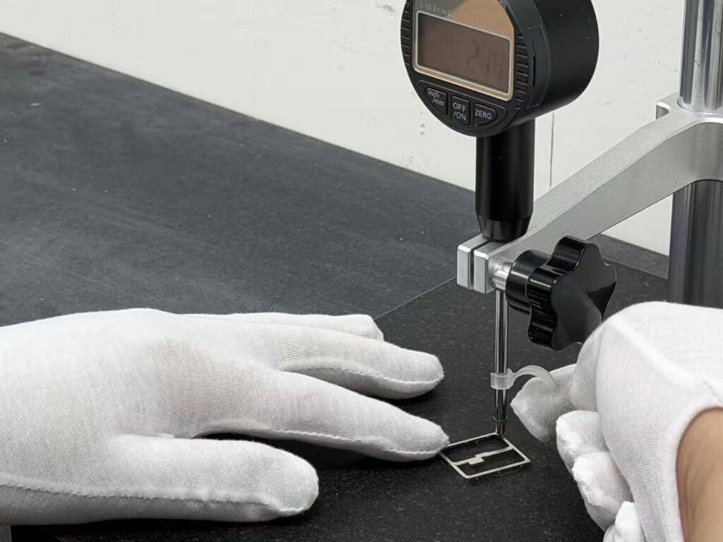
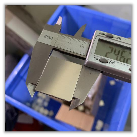
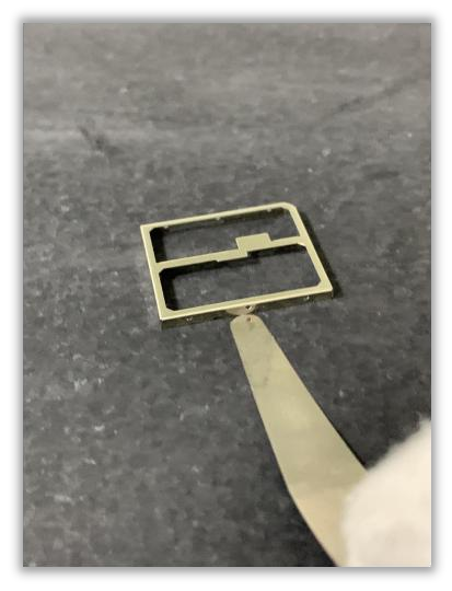
Whether we produce prototypes or run high-volume stamping, our inspectors use feeler gauges and high-precision height gauges to measure RF shield coplanarity. In addition, these inspections help us identify lifted edges early and maintain consistent dimensional accuracy throughout production.
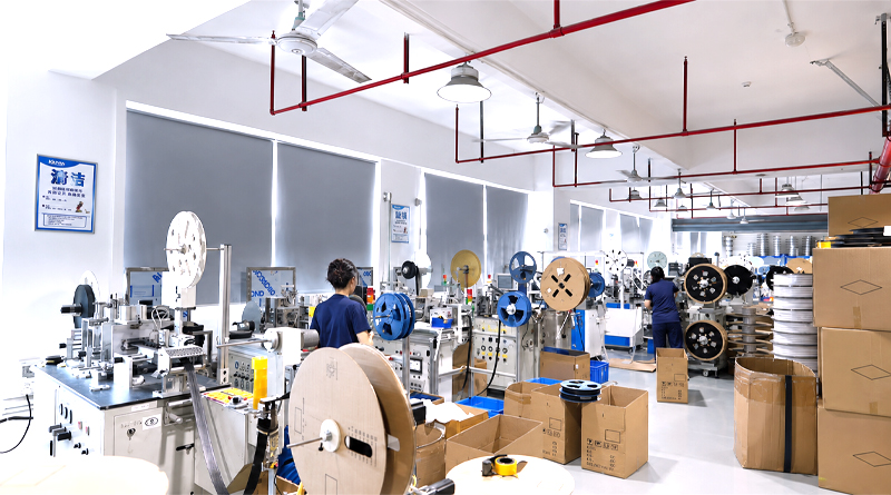
4.Tape-and-Reel Packaging and Tray Packaging
Tape-and-reel and tray packaging are the two most common packaging methods for RF shields. Generally, tape-and-reel packaging suits smaller, simpler shields that require automated SMT placement. In contrast, tray packaging provides better protection for large, complex, or deformation-prone shields.
6.FAQ
1.What thickness is commonly used?
A:Manufacturers commonly use material thicknesses from 0.10 mm to 0.30 mm for RF shield cans. Generally, smaller shields use thinner material, while larger or more complex shields require greater thickness or reinforcing ribs. However, the final choice depends on the material, dimensions, strength, flatness, and SMT requirements.
2.What Is the Difference Between an EMI Shield and an RF Shield?
A:An EMI shield protects electronic circuits from electromagnetic interference across a broad frequency range. In contrast, an RF shield mainly controls radio-frequency interference. However, buyers and manufacturers often use both terms interchangeably when describing PCB shielding cans.
3.What Drawing Files Do You Need?
Please provide a PDF, DWG, or DXF file for 2D dimensions and a STEP or IGES file for the 3D structure. Moreover, a PCB layout or Gerber file can help our engineers review component clearance and grounding areas. If you have no drawing, you can send us a physical sample for evaluation.

kaiyan